
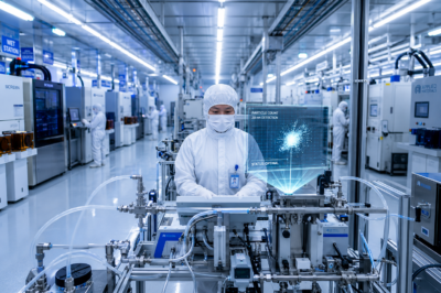
As semiconductor manufacturing pushes toward ever-smaller process nodes, ultra-fine particle monitoring is emerging as a critical line of defence against microscopic contamination, yield losses and billions of dollars in potential damage.
The semiconductor industry is entering an era in which the margin for manufacturing error has virtually disappeared. As chipmakers advance toward 5-nanometer, 3-nanometer and smaller process technologies, the battle for semiconductor reliability is increasingly being fought at a scale invisible to the human eye.
At the heart of this battle is something deceptively simple: a particle.
A speck of contamination that might once have been considered insignificant can now damage sophisticated semiconductor structures and potentially compromise an entire batch of high-value wafers. This is why 20-nanometer particle monitoring is gaining importance across modern semiconductor fabrication facilities, or fabs.
It is more than an improvement in measurement technology. It represents a fundamental change in how manufacturers approach liquid purity, contamination control and production quality.
The Microscopic Battlefield Inside a Chip Fab
Modern semiconductor manufacturing is an extraordinarily complex process. A silicon wafer can pass through hundreds of processing stages involving photolithography, etching, deposition, cleaning and chemical mechanical planarization.
During these operations, wafers are repeatedly exposed to ultrapure water and highly specialised process chemicals.
Any unwanted particulate matter in these fluids can become a potential source of a “killer defect”—a contamination event capable of rendering a semiconductor device electrically or physically defective.
At the 20-nanometer scale, the challenge becomes particularly demanding. Particles this small are extremely difficult to detect, quantify and eliminate. Conventional monitoring systems designed around larger particle thresholds may fail to identify early contamination trends, leaving manufacturers with a potentially costly blind spot.
The consequences can emerge much later, during wafer inspection or final electrical testing, when identifying the original source of the defect becomes significantly more difficult.
From 100 Nanometers to 20 Nanometers
The evolution of particle monitoring has closely followed the semiconductor industry’s relentless drive toward smaller device geometries.
As chip features have shrunk, contamination-control requirements have become increasingly stringent. A particle that posed little practical threat to an older generation of semiconductor devices can become a serious defect risk in today’s advanced manufacturing environment.
This has forced liquid particle counter technology to evolve.
Modern high-sensitivity systems use sophisticated laser-scattering techniques. A controlled fluid stream passes through an optical measurement region, where a precisely engineered light source interacts with particles suspended in the liquid.
The scattered light is captured by highly sensitive detectors and processed to determine particle size and concentration.
Detecting particles around 20 nanometers is an engineering challenge because the desired signal can be extremely weak compared with background optical and electronic noise. Advanced optics, highly controlled fluidics and sophisticated digital signal processing are therefore required to distinguish genuine particulate contamination from background signals.
Ultrapure Water: The Lifeblood of Semiconductor Manufacturing
Among the most critical fluids in a semiconductor fab is ultrapure water (UPW).
UPW is used extensively for cleaning and rinsing wafers throughout the manufacturing process. It must meet extraordinarily demanding purity requirements, with strict control over ions, organic compounds, microorganisms and particulate matter.
Monitoring particles at the 20-nanometer level provides manufacturers with significantly more detailed information about the condition of their UPW systems.
But water is only part of the equation.
Advanced semiconductor manufacturing also depends on numerous specialised chemicals used for etching, deposition, cleaning and other process steps. Maintaining the purity of these chemicals is equally important.
Chemical monitoring can be particularly challenging because some process fluids may be highly reactive, optically complex or otherwise difficult to analyse using conventional techniques.
High-sensitivity particle monitoring can help manufacturers detect contamination before it reaches critical process equipment, creating an additional layer of protection for the wafer.
Why Yield Matters So Much
In semiconductor manufacturing, technological sophistication ultimately translates into one crucial economic metric: yield.
Yield represents the proportion of functional devices produced from a wafer. Even a relatively small reduction in yield can have significant financial consequences in a high-volume manufacturing environment.
A contamination event can therefore be much more expensive than the cost of the particle-monitoring equipment itself.
This is where real-time monitoring becomes particularly valuable.
Instead of discovering contamination only after defective chips have been produced, fabs can use continuous particle-count data to identify abnormal trends and respond rapidly. This approach—often associated with excursion control—allows engineers to investigate a process before contamination develops into widespread product failure.
The monitoring data can also support root-cause analysis. If particle levels suddenly increase, engineers can investigate potential sources such as filters, pumps, valves, seals, piping or process equipment.
The objective is not simply to detect contamination.
It is to detect it early enough to prevent it from becoming a production crisis.
The Technology Behind 20-Nanometer Detection
Reaching the 20-nanometer monitoring threshold requires the integration of several technologies.
Advanced solid-state lasers and highly engineered optical systems provide the illumination needed to detect extremely small particles. At the same time, flow-cell design becomes critical.
The fluid must pass through the optical measurement zone in a controlled manner. Turbulence, bubbles and other disturbances can generate signals that resemble particulate contamination, potentially producing false alarms.
This is where software increasingly becomes as important as hardware.
Sophisticated signal-processing techniques—and, increasingly, machine-learning approaches—can help distinguish genuine particles from bubbles, molecular clusters and other sources of optical noise.
The result is a monitoring system capable not only of detecting extremely small signals but also of interpreting those signals intelligently.
That distinction matters because excessive false alarms can themselves become costly, triggering unnecessary investigations or production interruptions.
From the Fab to the Global Supply Chain
The importance of particle monitoring extends beyond semiconductor manufacturers.
The global semiconductor ecosystem includes chemical suppliers, equipment manufacturers, filtration companies, water-treatment specialists and process-control technology providers.
For all of these participants, increasingly stringent contamination requirements are creating a common language of purity.
As semiconductor demand continues to expand because of artificial intelligence, high-performance computing, 5G infrastructure, electric vehicles and autonomous systems, manufacturing consistency is becoming increasingly important.
A sophisticated chip is only as reliable as the manufacturing environment in which it is produced.
Consequently, advanced metrology and contamination monitoring are becoming important components of semiconductor supply-chain resilience.
The Next Frontier: 10 Nanometers and Beyond
The 20-nanometer threshold may not remain the industry’s ultimate frontier for long.
As semiconductor architectures become increasingly sophisticated, monitoring systems will face pressure to identify particles at even smaller scales. Research and development efforts are already looking toward increasingly sensitive detection technologies.
The trajectory is clear: as chip dimensions shrink, contamination-control requirements will become more demanding.
The future may therefore involve monitoring at 10 nanometers, 5 nanometers or potentially even smaller scales.
But the significance of 20-nanometer monitoring lies in what it represents today: a point at which optical engineering, fluid dynamics, semiconductor process control and advanced data analytics converge to protect some of the world’s most valuable manufacturing processes.
Precision Is the New Competitive Advantage
The semiconductor industry is often described in terms of processors, artificial intelligence, computing power and technological breakthroughs. Yet behind every advanced chip lies an enormous infrastructure dedicated to controlling things that are almost impossible to see.
Particle monitoring is one of those invisible technologies.
A 20-nanometer particle counter may never appear in the finished smartphone, computer or AI accelerator. Nevertheless, its role can be critical in ensuring that the device is manufactured reliably in the first place.
In the race toward smaller, faster and more powerful chips, the semiconductor industry is discovering an increasingly important principle:
The smaller the technology becomes, the greater the importance of controlling the smallest things.
At 20 nanometers, contamination control is no longer merely a quality-assurance exercise. It is a strategic manufacturing capability—one that can protect wafer yields, reduce production losses and help ensure the reliability of the digital infrastructure on which the modern world increasingly depends.







Leave a Reply